Contents
Introduction
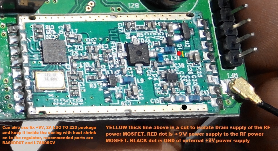
Ultimate LRS can easily be modded for 1W power using the mod described here, which simply changes the voltage on the OrangeRX modules.
But it’s possible to go much further : rcgroups user ‘Narpat‘ has made a lot of experimentation and invented a way to raise the output power to 2.7W with some modifications on the RFM23BP module itself.
Description
Original post
For all details please check his post in the ULRS thread here.
Videos
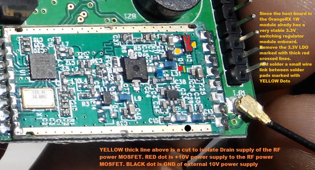
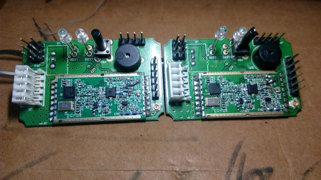
I realized that there is a small 3.3V LDO regulator chip in SOT-23 package on the RFM23BP module inside the OrangeRX 1W 433MHz module and there is another powerful 3.3V switching regulator module TSR-2433 available on the host board.
While looking at the datasheets of various SOT23 package 3.3V LDO’s I observed that for proper performance of the LDO, the input voltage should be atleast regulated voltage of the LDO for which its is rated + dropout voltage.
In this case I measured voltage output of the LDO and it was 3.15V, means the LDO was underperforming. To verify this fact, I just removed this LDO and soldered a small wire link between the input and output solder pads of the LDO.
Then I measured RF output at same 9V of the drain supply as per my previous mod of 2W, I was getting 2319mW instead of previous 2030mW.
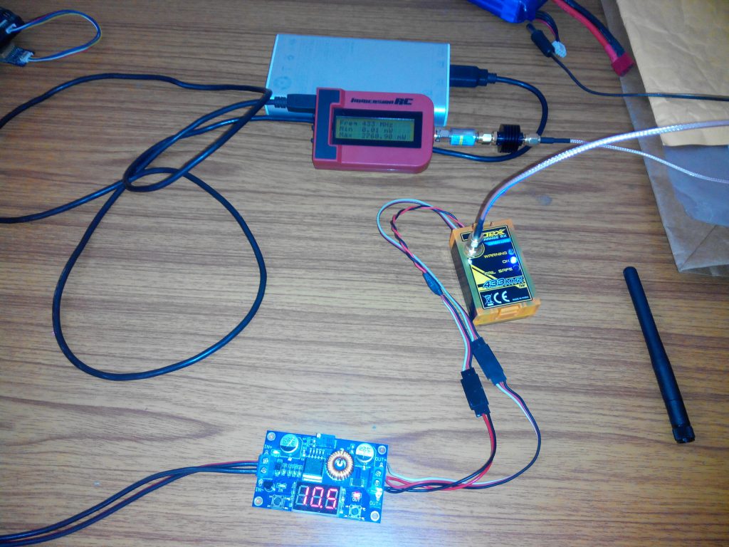
Then the increased the drain voltage of the RF power MOSFET, from 9V to 10V and got 2534mW. Kept it running throught the night and it was working perfect and the temperature was almost as previous.
So I would call it the ULRS 2.5W power mod.
I am also sharing pic of my IBCrazy style 433MHz open dipole antenna, I found its performance slightly better as compared with the original but that may be because I tuned it as per my requirement. This has slightly longer 50 ohm impedance rigid RF cable length and an additional option to mount on Skywalker or similar plane at suitable required location on the airframe.
Most of the RF Power MOSFET’s of different manufacturers of same package (PW-X) used in RFM23BP, are rated 10-12V and have maximum of 4Watt output. So it is not recommended to give more than 10V to the RF power MOSFET.
Since I have many modules so I could take chance of putting one module in risk by increasing the voltage upto 10.5V at which I got 2768mW.
Finally the RF power MOSFET got burnt at 10.8V, and running for one hour. So even 10.5V is not recommended, the safer side is maximum upto 10V, +/- 0.1V
While doing this mod, wear anti-static wrist band as MOSET’s are susceptible of getting damaged due to static charge.
Update 19th Feb 2016
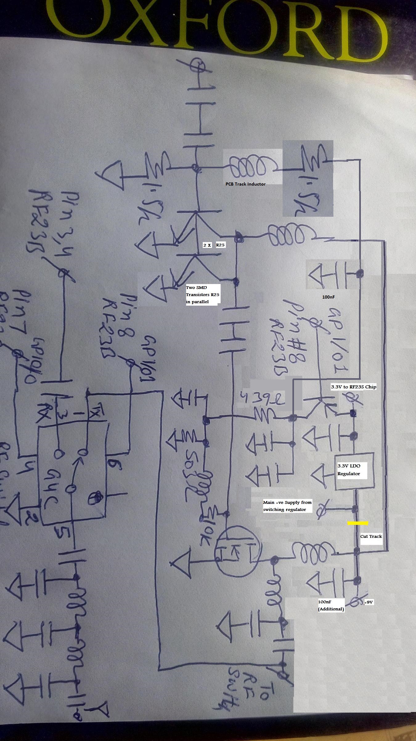
I have traced the entire RFM23BP board and made a rough hand drawn schematic, and found few design limitations like the RF switch can handle 1500mW input power. I have found some other RF switch chips with same footprints but which can handle much higher input power.
A PNP transistor controlling the gate bias of the RF power MOSFET, is being derived by GPIO_1 pin #8 of RF23S directly without any resistor in the path.
I might consider designing my own but a better one than this.
Update 22nd Feb 2016
The PNP transistor used for gate bias of RF power MOSFET is in SOT-323 (SC-70) package and have hfe (forward current gain) between 125 to 400 and the transistor has maximum collector current “Ic” of 100mA.
In present configuration this transistor can attain maximum collector current of 3.5mA due to two series resistors 503 ohm + 439ohm = 942ohm connected from collector to GND. GP I/O’s RF23S chip on the RFM23BP module outputs VDD-0.6V on high level.
Considering minimum hfe of 100, theoretically the base resistor value is coming out at 77K ohm but there is no option on the PCB to incorporate this base resistor.
In one of my module where I given 3.6V externally to the chip RF23S, and run for long time, this PNP transistor was actually damaged by the chip’s (RF23S) high I/O voltage and due to no base resistor.
I was surprised to see that there was no RF output, lateron by tracing and testing the transistor, I found it faulty which always tied the gate of the RF MOSFET to GND and not allowing to amplify anything.
For a new design, its must a minimum of 10k resistor and this PNP transistor be in slightly bigger package SOT-23.
Update 20th June 2017
There is update in the traced hand sketch schematic of the RFM23BP module. Collector of the PNP bias transistor (which switches on – off the RF power MOSFET), also goes to the base of RF driver NPN transistor with SMD marking “R25”, via 1.5K ohm resistor and then an inductor (created on the PCB via copper track).
There is also a 100nF capacitor connected between the collector of the miniature PNP bias transistor and GND.
Now, with this information, I reaches the conclusion that this miniature PNP has and additional load of +ve biasing the RF driver transistor R25.
Any regular TO-92 package BC556, BC557 transistors can be used to achieve the functionality of this miniature PNP bias transistor but this would require some small wiring.
With this new information, it has also become clear that RF driver transistor(s) are not operating in Class-C but just in Class-A only.
Due to time issue I am unable to devote much and came house today evening only and have to rush out tomorrow again. Once I again reaches back, I would possibly suggest optimum modification.
Update 21st June 2017
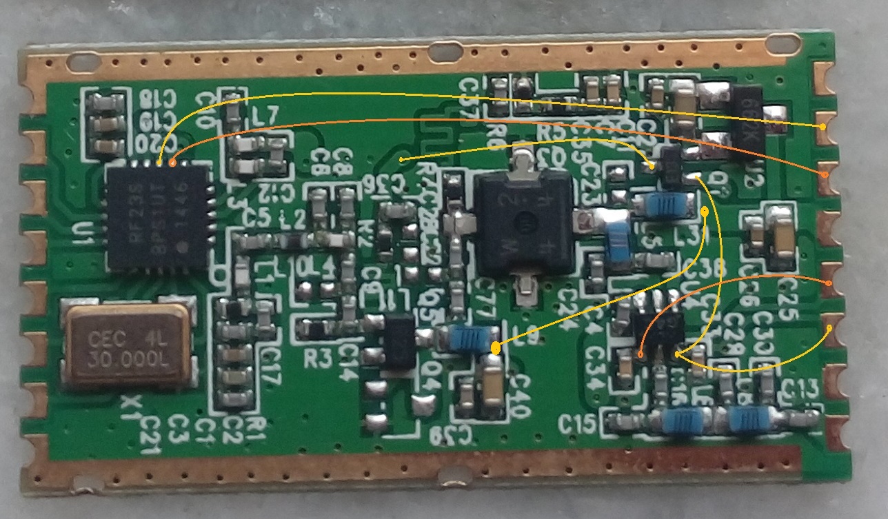
I have added two images here and to my main old post. These give more details about the schematic on the PCB.
The other image shows how to use BC556 or BC557 TO-92 package transistor as an alternative to miniature PNP transistor.I have given general idea, its upto the user, where to place the through hole to-92 package transistor BC557 on the board but one thing must be kept in mind is to keep it away from RF power MOSFET and its output inductors in order to prevent parasitic value change of RF components and to avoid RF injection on the base of the transistor.
Update 22nd June 2017
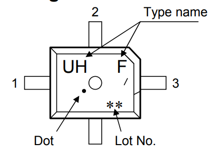
The SMD marking on the RF power MOSFET on few of my boards, I observed long back was W 2 2 Z, see the image attached.
After looking at the datasheet posted by Ben.it seems HopeRF guys did yet another design mistake, they forgot to put 39pf capacitor from gate of the RF power MOSFET to GND which is must as per the application schematic @450MHz. This is needed to match the complex input impedance of the RF Power MOSFET.
I have suggested a location to solder this missing 39pf cap but I am not sure, how much would it improve RF output power.
The fundamental reason of R25 getting hot in RFM23BP boards of most users is the 1.5K resistor via which the driver NPN transistor R25 gets +ve bias from the miniature PNP transistor.50% of Vcc means 3.3V/2 = 1.65V is the +ve bias voltage the R25 transistor gets on its base when TX is on means miniature PNP transistor switches on. During TX on period, 2.1mA current flows through the base – emitter junction. Let us assume a practical hfe value of 250, that case collector current would like to go upto a value = input current X hfe = 525mA. Oh my God, that’s hell lot of current ! which is making it hot.
With present bias resistor of 1.5K, we just can not make the +ve power supply of the driver transistor R25, common with RF MOSFET which can go upto 10V. We have to change this resistor to a higher value maybe 10K.
Update 27th June 2017
I have observed in two fresh RFM23BP modules that the SMD marking on the tiny bias PNP transistor is E13 and it’s part number is DTA143ZKA and package is SOT-723 (measured with digital vernier caliper) .
It is surprising to see the datasheet that Tiny bias PNP transistor having SMD marking E13 has inbuilt two resistors, see the image attached below. This has turned around the observation about this transistor. The resistor is already present then why this transistor is getting damaged ?
For those who says we are happy with 800-1000mW RF output power of the ULRS, refer this mod image, its self explanatory.
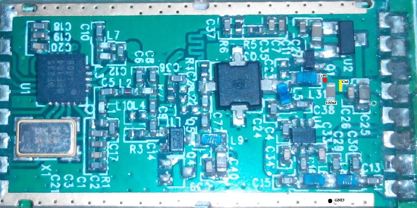
1. Cut the track carefully with fine knife by viewed under enlightened lens.
2. Solder another R25 in parallel and use 4.7K series resistor which goes to collector of PNP bias transistor in place present 1.5K.
3. Solder 39pF and 100nF cap as per shown in the attached image.
4. Connect +5V, 2A regulated power at the pad towards RF power MOSFET before the track cut, refer attached image. Use external switching regulator for this.
Test it for more than 24Hrs, if no issue observed (observe temperature of both R25 transistors), its done !
By using 10K inplace of 4.7K and replacing +5V by +9V, you will get 1500-2000mW and 2000-2500mW with +10V
If you do not need more than 800-1000mW then don’t go beyond +5V.
Datasheets
- RF MOSFET of RFM23BP module : Toshiba RFM07U7X
- Datasheet
- Toshiba RF Semiconductors catalog with more information about this Mosfet on page 7.
- ba90dd0t-9v-2a-ldo
- l78s09cv-9v-2a-ldo
- mcp1702-3-3v-ldo-sot-23-package
- bc856w-sot-323-pnp-transistor
- More datasheets are available in the original post in ULRS thread here.
Photos and schematics
Schematics and photos made by rcgroups user Narpat, edited on June 28th 2017. See his post for full details.
Quick 2W power mod :

